Comments
- No comments found

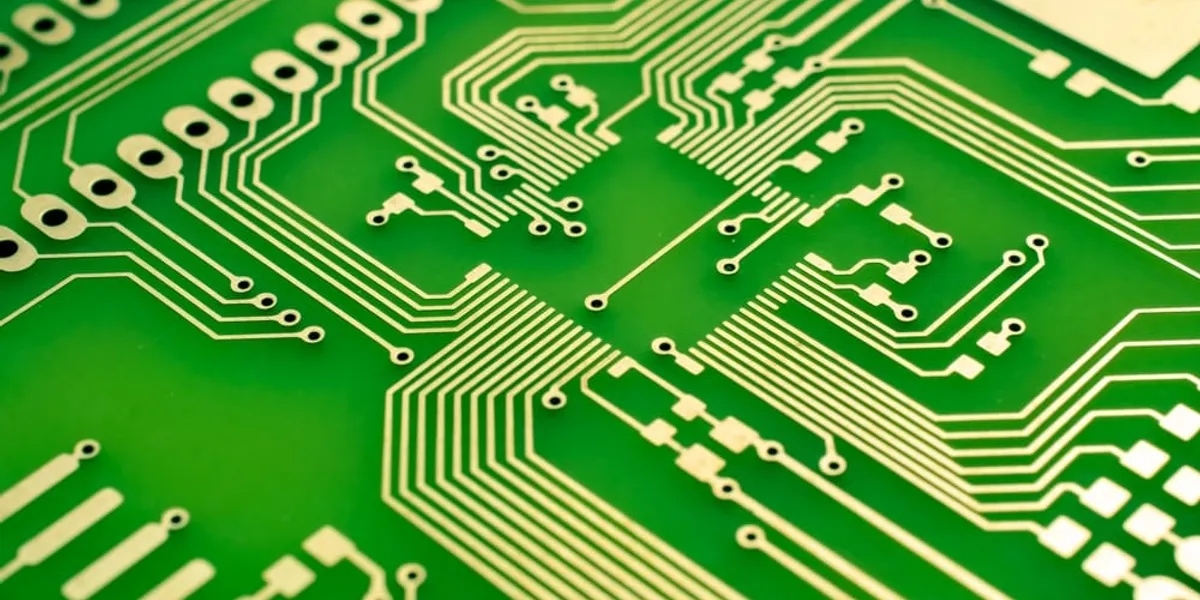
PCB refers to ‘printed circuit design’ and acts as an innovative piece of technology that helps bring electrical circuits to life.
Using copper conductors to connect electrical components, PCBs offer mechanical support to mount your chosen device.
You’ll find many conductive features on a PCB, such as copper pads, traces, and conductive planes. The entire structure is designed using insulating materials, which lie between conductor layers.
PCB design has become prominent within the electronics industry and plays a fundamental role in providing electrical connections between varying components.
When coming up with your PCB design, it’s important to consider where you want components placed on the board, and where the board will sit amongst other circuits. Placement should be carefully considered to avoid expensive rework and time wasting.
Firstly, the components that have similar functions should always be grouped together. For instance, your power management elements should be in the same section. These are typically the components that develop the most heat and generate high currents.
To simplify your PCB layout, you’ll need to ensure that your integrated circuits are all aligned. This is to make the assembly process more efficient, whilst reducing positioning errors.
Don’t forget that the areas of your PCB which contain analogue, digital, radio frequency or power components should all be kept separate from one another. This is to prevent any high-risk interference between signals.
It’s important to consider the limitations of your circuit to ensure you are creating a safe and functioning board at the end of your project.
Power planes are an important feature of your PCB. They should be carefully analysed to determine how large they need to be and what current are they capable of carrying.
Whilst power and ground planes offer multiple purposes to your PCB design, they’re a key component and require the same level of detail as every other element in your layout.
To find out your power plane’s current capacity, you’ll need to know the maximum allowed temperature rise from the external ambient temperature, the required current and the copper weight of the power plane. That way, you can ensure your entire PCB design will remain reliable.

PCB design uses traces to connect each component, and the width of these traces is dependent on three separate factors:
Current: The level of current carried through the trace will determine the minimum width required to prevent it from overheating. The higher the current, the wider the trace will need to be.
Manufacturability: Traces can’t be reliably manufactured if they’re too thin. You’ll likely be working with larger trace widths than the manufacturer can typically produce.
Impedance: Digital or radio frequency signals will require a specific trace width to hit a specific impedance value, however, this doesn’t apply to all.
BBN Times connects decision makers to you. Experts in their fields, worth listening to, are the ones who write our articles. We believe these are the real commentators of the future. We quickly and accurately deliver serious information around the world. BBN Times provides its readers human expertise to find trusted answers by providing a platform and a voice to anyone willing to know more about the latest trends. Stay tuned, the revolution has begun.
Leave your comments
Post comment as a guest